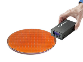
Cognex machine vision solutions are essential to every step of the semiconductor device manufacturing process, from wafer fabrication to integrated circuit (IC) packaging and mounting. Cognex tools handle a range of integrated circuit (IC) package types, including leaded parts, system-on-chip (SoC), and microelectromechanical system (MEMS) devices and provide traceability throughout assembly. Vision tools locate features of wafers, dies, and packages under extremely challenging conditions and can detect low contrast and noisy images, variable fiducial patterns, and other part variations.
Cognex supports a wide range of applications in the wafer and semiconductor device manufacturing process, including:
Machine vision performs alignment, inspection, and identification to help manufacture high quality wafers used in integrated circuits (ICs) and other semiconductor devices. Machine vision automates wafer handling, enables precision alignment, inspects bond pads and probe tips, and can measure critical dimensions of crystalline structures.